非破壊検査システム
NONDESTRUCTIVE INSPECTION SYSTEMS
ピックアップ
HOT TOPICS
製品を探す
FIND PRODUCTS
-
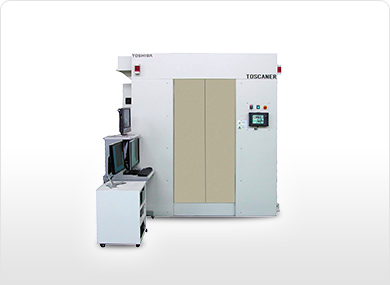
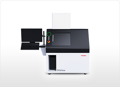
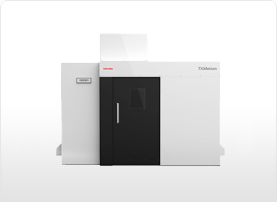
TOSCANER-24500twin/AV
TOSCANER-34500FD高エネルギーCTスキャナ
管電圧 : 450kV
焦点 : 0.4mm/1mm用途
大型アルミダイカスト 鉄 鋳物 シリンダー/タイヤ/エンジンブロック
-
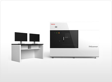

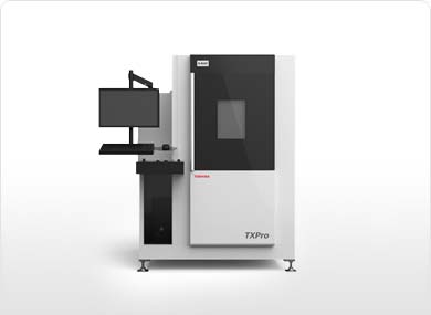
TXS-33000FD/32300FDマイクロCTスキャナ
管電圧 : 300kV/230kV
焦点 : 4μm用途
小型電子部品 実装基板 アルミダイカスト 電池 モールド品 樹脂 繊維 GFRP/CFRP他
-
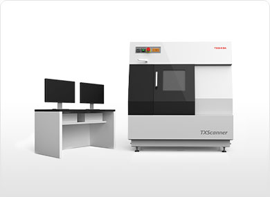
TXS-31300FD/30900FDコンパクトCTスキャナ
管電圧 : 130kV/90KV
焦点 : 5μm用途
小型電子部品 モールド品 樹脂 繊維 GFRP/CFRP他
-

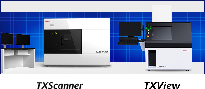
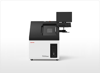
TXV-S4130FD/S4090FDスタンダードモデル・X線検査装置
管電圧 : 130kV/90kV
焦点 : 5μm用途
実装基板 BGA(半田ボール) 電子部品 デバイス センサー 樹脂
-
TXV-CH4090FD小型傾斜モデル・X線検査装置
管電圧 : 90kV
焦点 : 5μm用途
実装基板 BGA(半田ボール) 電子部品 デバイス センサー 樹脂
-

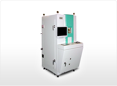
TXP-5150FDX線検査装置
管電圧 : 150kV
焦点 : 0.1mm用途
アルミダイカスト部品 機械部品 電気部品 樹脂成型品
-
X's-PRO
インライン/オフライン
自動検査/手動検査用途
アルミホイール検査 エンジンカバー検査 パワーモジュール検査 実装基板検査用
-
X's-BT
インライン
用途
二次電池(リチウムイオン電池)
-

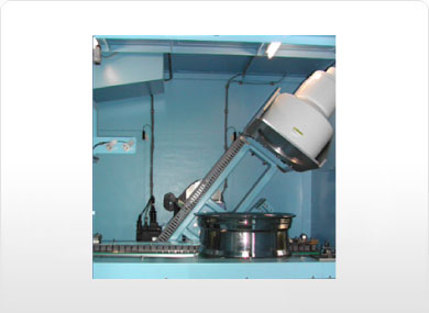
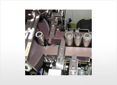
高速度X線透視検査システム
製品内部の挙動を可視化用途
精密機械の落下時の内部検査 電気/電子部品の損傷過程解析&機構部
動作部の挙動観察 流体/紛体の挙動観測、溶接現象観察etc -
X's OFFLINE
X線透視検査装置
手動検査用途
電気部品 電池 アルミダイカスト部品 実装基板
-
SU
結晶方位測定装置
用途
結晶種類 : Si、GaAs、サファイアなど 測角方位 : Vノッチ・オリフラ方位、カット
面方位